当前位置:首页 > 产品中心
产品中心

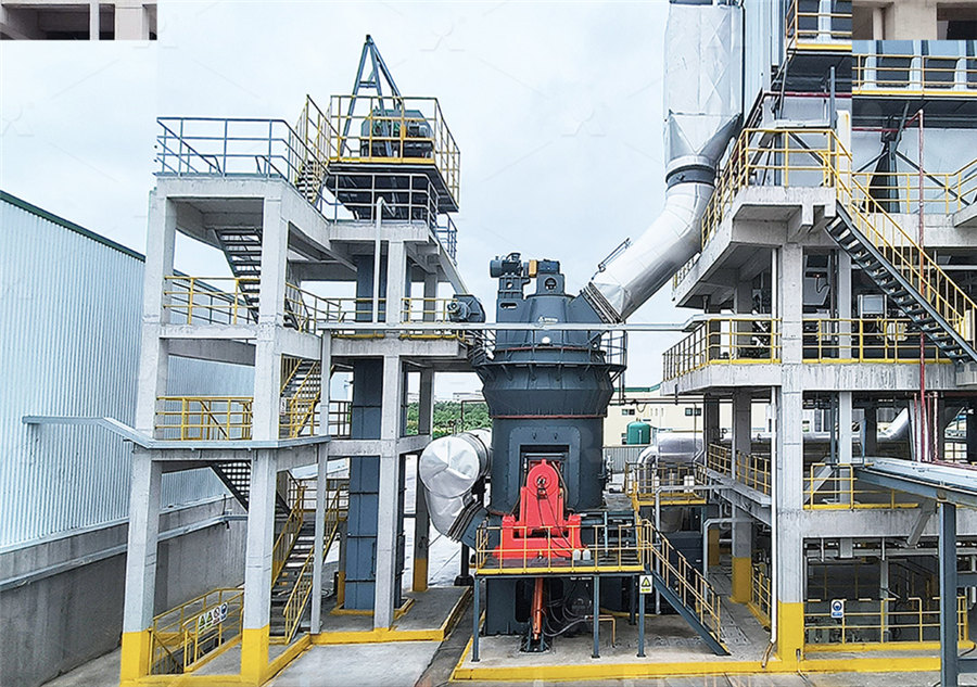
Backgrinding Machine Sorece
浅析晶圆背面研磨工艺 ROHM技术社区 eefocus
2023年9月1日 经过前端工艺处理并通过晶圆测试的晶圆将从背面研磨(Back Grinding)开始后端处理。 背面研磨是一项关键工序,不仅旨在减小晶圆的厚度,还能有效解决前后两个工艺之间可能出现的问题。 随着半导体芯 2023年4月17日 经过前端工艺处理并通过晶圆测试的晶圆将从背面研磨(Back Grinding)开始后端处理。 背面研磨是将晶圆背面磨薄的工序,其目的不仅是为了减少晶圆厚度,还在于联结 半导体制造技术:背面研磨(Back Grinding)决定晶圆的厚度2018年7月6日 在许多IC 工艺后期都会进行晶圆背面研磨(Backside Grinding, BG),使晶圆薄形化,以利后续晶圆切割及封装等。 例如:在智能卡应用上,必须将晶圆厚度由700~600μm 研磨 晶圆背面研磨与湿式刻蚀应力消除工艺2023年5月15日 背面研磨具体可以分为以下三个步骤:、在晶圆上贴上保护胶带贴膜(Tape Lamination);第二、研磨晶圆背面;第三、在将芯片从晶圆中分离出来前,需要将晶圆安置在保护胶带的晶圆贴片(Wafer Mounting)上 晶圆背面研磨(Back Grinding)工艺介绍合明科技3 天之前 Wafer backgrinding is the first step in semiconductor packaging, the process of encasing one or more discrete semiconductor devices or integrated circuits (IC) for protection Known also as wafer thinning or wafer lapping, Wafer Backgrinding and Semiconductor 2019年2月4日 Current practice is to use vacuum or an adhesive tape to secure the wafer to the chuck, and reduce the thickness by grinding As illustrated in Figure 1, a standard back grinder Semiconductor BackGrinding IDCOnline
.jpg)
背面研磨的过程控制解决方案 Marposs
晶圆背面研磨(或晶圆减薄)是半导体生产中的一道重要工序,此工序需要严格控制晶圆厚度,使晶圆达到超薄的厚度,最终可叠放和高密度封装在微型电子器件中。 晶圆减薄是半导体生产 2024年10月5日 Backgrinding involves grinding the backside of a silicon wafer to reduce its thickness The process typically works as follows: The front side (circuit side) of the wafer is The Backgrinding Process: A Key Step in Semiconductor 2025年1月17日 backgrinding, where a grinder is typically employed as the equipment The processing quality of backgrinding is evaluated using indices such as TTV (Total Thickness Governing Factors of Processing Quality for the Silicon DESCRIPTION Achieving the correct wafer thickness before assembly is a key factor in semiconductor manufacturing Wafer back grinding (or wafer thinning) is a semiconductor manufacturing process designed to control the wafer Back Grinding: Wafer Thinning Marposs2025年5月6日 Full Auto Dicing Saw Machine ADS200A 1 Full Auto Back Grinding Machine VRG300A 게시물 검색 검색대상 개인정보취급방침 이메일주소무단수집거부 에이엠테크놀로지 에이엠테크놀로지 (주)3 天之前 Wafer backgrinding, or wafer thinning, is an essential semiconductor service designed to reduce wafer thickness to integrate and package circuits in smaller electronic devices Syagrus Systems is an experienced provider of Silicon Wafer Backgrinding Wafer Thinning
Back Grinding Machine by 에이엠테크놀로지(주) 코머신
CMP Machine (Double Side Process) ADP1200FD CMP 1 / 2 에이엠테크놀로지(주) Biz Home 파인 그라인딩, 다이싱, 래핑, 폴리싱, 슬라이싱, 슬롯 연삭기 제조업체 1994년 알파정공을 모태로 In this study, we investigated the characteristics of the ntype Ni/SiC ohmic contact using the laser annealing process on thin wafers The electrical behavior of the ohmic contacts was tested in Thickness of the SiC wafer prior to and after grinding2023年5月22日 晶圆背面研磨(Back Grinding)工艺简介经过前端工艺处理并通过晶圆测试的晶圆将从背面研磨(Back Grinding)开始后端处理。背面研磨是将晶圆背面磨薄的工序,其目的 晶圆背面研磨(Back Grinding)工艺简介 制造/封装 电子 1 최종목표 Multi Head LED Wafer Back Grinding Machine의 양산 System 개발2 개발내용 및 결과1) 기존의 Back Grinding System의 Single Head Type을 Multi Head Type으로개선 1개의 [보고서]Multi Head LED Wafer Back Grinding Machine 개발 In recent years, the demand for ultrathin die for use in mobile phones, stacked packages, and a myriad of other applications has been increasing DISCO delivers complete ultrathin grinding Grinding Solutions DISCO Corporation5 天之前 The HVG Series Vertical Grinding Machine is designed to grind advanced materials to a high degree of precision in flatness and surface quality, often reducing or eliminating the HVG Wafer Grinder Series Engis
.jpg)
Wafer Backgrind eesemi
2019年8月14日 Wafer backgrinding has not always been necessary, but the drive to make packages thinner and thinner has made it indispensable Most package types in the Wafer grinding is a process used in the semiconductor manufacturing industry to reduce the thickness of wafers and improve their flatness The process involves grinding the wafer Grinding Equipment Semiconductor Materials and Equipment2025年1月2日 Semiconductor BackGrinding The silicon wafer on which the active elements are created is a thin circular disc, typically 150mm or 200mm in diameter During diffusion and Semiconductor Back Grinding PDF Wafer (Electronics)4 天之前 Model GDM300 grinder is a fully automatic continuous downfeed grinding machine with dual polishing stations for increased throughput Wafers are handled through the machine by a 6axis robot, and load/unload arms OKAMOTO GDM300晶圆抛光/晶圆背抛 上海衡鹏2023年7月11日 Wafer backgrinding is a crucial step in semiconductor manufacturing, as it prepares the wafer for further processing and packaging The procedure comprises the Wafer Backgrinding: An InDepth Guide to SemiconductorTherefore, a modern wafer grinding machine begins with a coarse grinding wheel to get a fast removal of the silicon and at the end follows a fine grinding process step with small grit size Fast and precise surface measurement of backgrinding silicon
.jpg)
Back Grinding Machine DG Division
2025年5月5日 Full Auto Back Grinding Machine VRG300A 게시물 검색 검색대상 AM Technology Co, Ltd Address: 174, Asanvalleyjungangro, Dunpomyeon, Asansi, Achieving the correct wafer thickness before assembly is critical in semiconductor manufacturing Wafer back grinding (or wafer thinning) is a semiconductor manufacturing process designed to Solutions for back grinding process control MarpossA back grinder is a machine used in semiconductor manufacturing to grind the back of wafers to a uniform thickness This is typically done after the wafers have been cut from a larger Back Grinder Semiconductor Materials and Equipment2023年5月22日 【半导光电】晶圆背面研磨(BackGrinding)工艺简介 今日光电 18:00 从周级到天级:云仿真加速实战 STM32开发板、小米手环、华为耳机,等你来赢! 今日光电 【半导光电】晶圆背面研磨(BackGrinding)工艺简介 电子 2021年12月21日 semiconductor wafers Matched Grinding Machine: Japanese, German, American, Korean and Chinese grinders Good TTV and less damage section 减薄砂轮主要用 背面减薄砂轮 China Abrasives2023年1月16日 129 backgrinding machine is used, with installed UV curing and de taping process up to wafer 130 mounting, for all the three evaluation wafers The BG machine have Backgrinding Tape Selection Analysis for Adhesion
Semiconductor Grinding, Lapping, Polishing
5 天之前 The HVG Series Vertical Wafer Grinding Machine is designed to grind advanced materials to a high degree of precision in flatness and surface quality, often reducing or eliminating the need for lapping Watch Video Technical 2024年5月1日 schemes of grinding machine, in which the red curve represents the wheel grinding edge The configuration illustrated in Figure3a was proposed by Tonshoff et al [10] Optimization in the Wafer Backside Grinding Process2023年4月17日 经过前端工艺处理并通过晶圆测试的晶圆将从背面研磨(BackGrinding)开始后端处理。背面研磨是将晶圆背面磨薄的工序,其目的不仅是为了减少晶圆厚度,还在于联结前 半导体制造技术:背面研磨(Back Grinding)决定晶圆的厚度Intech specializes in providing cuttingedge wafer thinning services to unlock the full potential of your semiconductor devices With our stateoftheart capabilities for 12inch wafers, we offer Silicon Wafer Back Grinding/Wafer Thinning Services IntechThe wafer backside grinding process has been a crucial technology to realize multilayer stacking and chip performance improvement in the three dimension integrated circuits (3D IC) Illustration of wafer backside grinding (a) Diagram of in 2024年4月24日 根据QY Research(恒州博智)的统计及预测,2023年全球晶圆背面研磨机市场销售额达到了 亿美元,预计2030年将达到 亿美元,年复合增长率(CAGR)为 %(2024 20242030全球与中国晶圆背面研磨机市场现状及未来发展趋势
Home Ulmer Werkzeugschleiftechnik GmbH
Our grinding machines cover the entire process chain of the tool Precise and effective CNC control and drive systems from NUM as well as unified, graphically supported user interface backgrinding (thinning) the wafer down from 725 microns thick in the case of 200mm wafers, and 775 microns thick in the case of 300mm wafers, down to approximately 150 microns or less Technology Transfer for MEMS and Advanced PackagingChina Back Grinding Machine wholesale Select 2025 high quality Back Grinding Machine products in best price from certified Chinese Machine Supplies manufacturers, Z Machine China Back Grinding Machine, Back Grinding Machine DESCRIPTION Achieving the correct wafer thickness before assembly is a key factor in semiconductor manufacturing Wafer back grinding (or wafer thinning) is a semiconductor manufacturing process designed to control the wafer Back Grinding: Wafer Thinning Marposs2025年5月6日 Full Auto Dicing Saw Machine ADS200A 1 Full Auto Back Grinding Machine VRG300A 게시물 검색 검색대상 개인정보취급방침 이메일주소무단수집거부 에이엠테크놀로지 에이엠테크놀로지 (주)3 天之前 Wafer backgrinding, or wafer thinning, is an essential semiconductor service designed to reduce wafer thickness to integrate and package circuits in smaller electronic devices Syagrus Systems is an experienced provider of Silicon Wafer Backgrinding Wafer Thinning
.jpg)
Back Grinding Machine by 에이엠테크놀로지(주) 코머신
CMP Machine (Double Side Process) ADP1200FD CMP 1 / 2 에이엠테크놀로지(주) Biz Home 파인 그라인딩, 다이싱, 래핑, 폴리싱, 슬라이싱, 슬롯 연삭기 제조업체 1994년 알파정공을 모태로 In this study, we investigated the characteristics of the ntype Ni/SiC ohmic contact using the laser annealing process on thin wafers The electrical behavior of the ohmic contacts was tested in Thickness of the SiC wafer prior to and after grinding2023年5月22日 晶圆背面研磨(Back Grinding)工艺简介经过前端工艺处理并通过晶圆测试的晶圆将从背面研磨(Back Grinding)开始后端处理。背面研磨是将晶圆背面磨薄的工序,其目的 晶圆背面研磨(Back Grinding)工艺简介 制造/封装 电子 1 최종목표 Multi Head LED Wafer Back Grinding Machine의 양산 System 개발2 개발내용 및 결과1) 기존의 Back Grinding System의 Single Head Type을 Multi Head Type으로개선 1개의 [보고서]Multi Head LED Wafer Back Grinding Machine 개발 In recent years, the demand for ultrathin die for use in mobile phones, stacked packages, and a myriad of other applications has been increasing DISCO delivers complete ultrathin grinding Grinding Solutions DISCO Corporation5 天之前 The HVG Series Vertical Grinding Machine is designed to grind advanced materials to a high degree of precision in flatness and surface quality, often reducing or eliminating the HVG Wafer Grinder Series Engis
Wafer Backgrind eesemi
2019年8月14日 Wafer backgrinding has not always been necessary, but the drive to make packages thinner and thinner has made it indispensable Most package types in the